 AETHERIUM
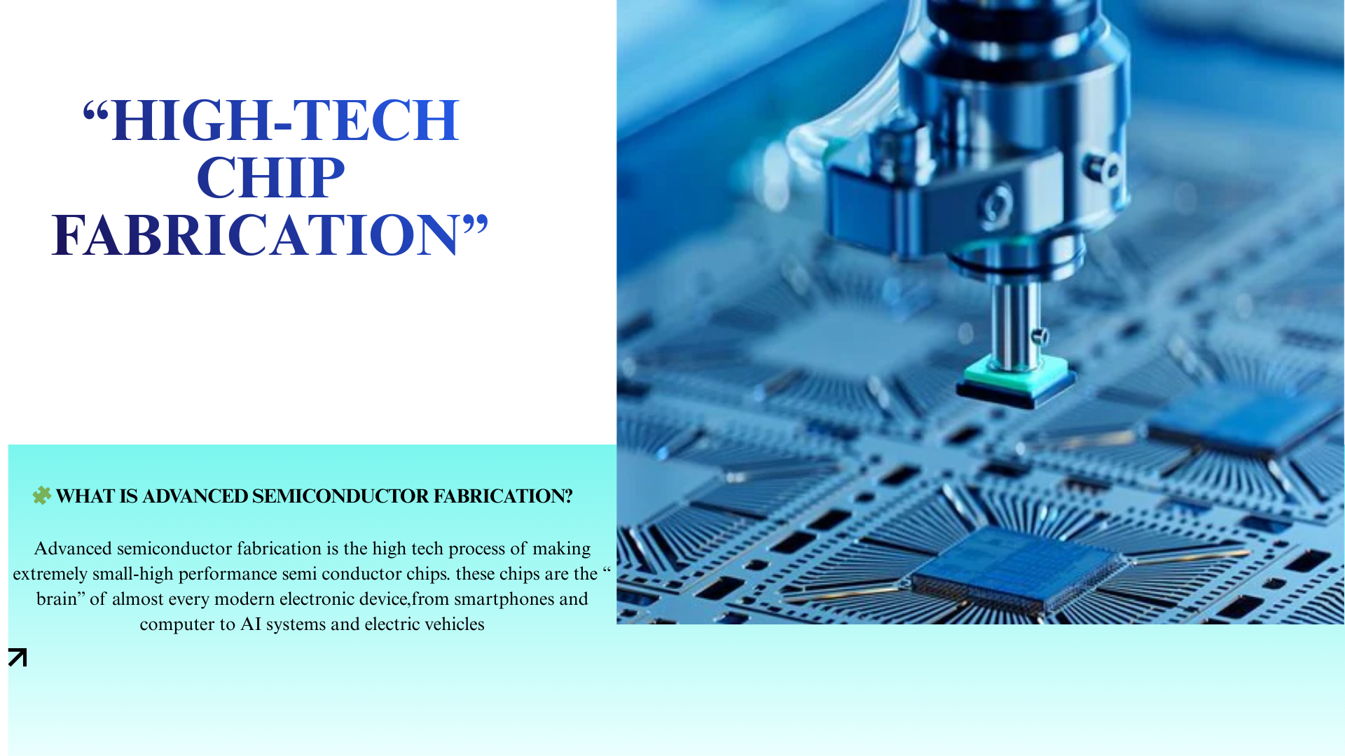
What is Advanced Semiconductor Fabrication?
Advanced semiconductor fabrication refers to the high-precision manufacturing of microchips using techniques that allow for nanometer-scale circuits on semiconductor wafers. Unlike early methods, modern fabrication can create billions of transistors on a single chip, enabling powerful computing capabilities while reducing energy consumption and physical size.
The process involves multiple stages, including photolithography, deposition, etching, doping, and packaging, to transform a silicon wafer into a fully functional chip. These chips serve as the heart of electronic devices, controlling everything from data processing to wireless communication.
Key Processes in Semiconductor Fabrication
1. Wafer Preparation
Semiconductor chips are built on silicon wafers, which are sliced from highly pure silicon ingots and polished to a mirror finish. These wafers provide a smooth and stable platform for circuit construction.
2. Photolithography
This is a critical step where a light-sensitive photoresist is applied to the wafer. Ultraviolet light transfers the circuit pattern from a mask onto the wafer, defining the microchip’s intricate design.
3. Etching
Etching removes unwanted material from the wafer according to the pattern created during photolithography. Both wet etching and dry (plasma) etching are used depending on the precision required.
4. Doping
Doping introduces specific impurities into the silicon to alter its electrical properties, creating regions of p-type and n-type semiconductors, which are essential for transistor function.
5. Deposition
Material layers, such as metals or insulators, are deposited on the wafer using techniques like Chemical Vapor Deposition (CVD) or Physical Vapor Deposition (PVD) to form interconnects and insulation layers.
6. Chemical Mechanical Planarization (CMP)
CMP smooths the wafer surface after deposition and etching to ensure uniform layers, which is crucial for high-density chip fabrication.
7. Packaging and Testing
After fabrication, wafers are sliced into individual chips, packaged to protect circuits, and rigorously tested to ensure functionality and reliability before integration into electronic devices.
Materials Used in Advanced Semiconductor Fabrication
Silicon – The primary material for wafers due to its excellent semiconducting properties.
Metals – Copper and aluminum are used for wiring and interconnections.
Insulators – Silicon dioxide and other dielectric materials isolate components.
Photoresists – Light-sensitive chemicals used in photolithography.
Dopants – Elements like boron and phosphorus modify electrical conductivity.
Advantages of Advanced Semiconductor Fabrication
Miniaturization – Enables smaller, lighter, and more powerful devices.
High Performance – More transistors per chip allow faster processing.
Energy Efficiency – Reduces power consumption in electronic devices.
Reliability – Advanced processes produce highly consistent and durable chips.
Innovation – Supports emerging technologies like AI, 5G, and autonomous systems
Challenges in Advanced Semiconductor Fabrication
High Cost – EUV machines and cleanroom facilities are extremely expensive.
Complexity – Nanometer-scale fabrication requires precise control and advanced equipment.
Material Limitations – New materials are needed for next-generation chip performance.
Yield Issues – Defects in wafer processing can reduce the number of usable chips.
Environmental Impact – Semiconductor manufacturing consumes significant energy and chemicals
Future Trends
Sub-3nm Fabrication – Pushing limits of Moore’s Law with smaller transistors.
3D and Heterogeneous Integration – Stacking chips of different types for enhanced functionality.
Quantum and Neuromorphic Chips – Next-generation chips for AI and quantum computing.
Sustainable Manufacturing – Reducing energy consumption and waste in semiconductor fabrication